Plenary Speakers
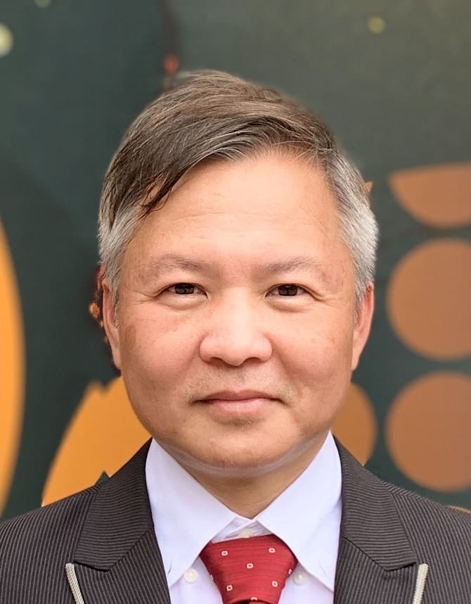
Chair Prof. and Department Chair, Ying-Hao Chu
Department of Materials Science & Engineering,
College of Semiconductor Research (joint),
National Tsing Hua University, Taiwan
Title of Plenary Speech
To be announced
Abstract of Plenary Speech
To be announced
GlobalFoundries Chair Prof. Cheng-Kuo Lee
Center for Intelligent Sensors and MEMS, National University of Singapore, Singapore
Department of Electrical and Computer Engineering, National University of Singapore, Singapore
National Centre for Advanced Integrated Photonics, Singapore
Title of Plenary Speech
CMOS Photonics Circuits Enabled Photonic Neural Networks and Edge AI Sensing
Abstract of Plenary Speech
With the growing demand for energy-efficient AI applications, the rapid development of photonic neural networks (PNNs) represent a strategy for integrating photonics with AI computing architectures. PNNs harness multiple degrees of freedom of light, i.e., wavelength, amplitude, phase, mode, and polarization, to encode and manipulate large volumes of data in parallel. Through optical multiplexing, PNNs enable high-throughput, low-latency computation while reducing energy consumption compared with electronic counterparts. The development of AlN/Si-based CMOS photonics circuits have been developed as a near-sensor edge computing (NSEC) platform which pushes the boundary of real-time AI by combining electro-optic microring resonators (MRRs) and thermo-optic interferometers (MZIs) to achieve low-latency neural computation directly at the sensing layer. Demonstrated with high accuracy in multimodal gesture and gait classification tasks (96.77% and 98.31%, respectively), and achieving latency under 10 ns with energy consumption below 0.34 pJ, such platforms are paving the way for privacy-preserving, always-on AI hardware for healthcare, robotics, and immersive interaction systems. Overall, the fusion of AI-enhanced photonic sensing, on-chip neuromorphic computing, and flexible sensor integration represents a paradigm shift for future edge AI sensing systems. As optical edge computing continues to mature, it will become a cornerstone in the transition from centralized cloud AI to energy-efficient, responsive, and context-aware edge intelligence. Looking ahead, the convergence of AI, photonic integration, and edge computing will catalyze the next wave of intelligent systems that are no longer confined to centralized data centers or limited by power and latency bottlenecks. Future edge AI sensing architectures will evolve toward using CMOS photonics circuits enabled computing and sensing integrated chips which can achieve perception, inference, and adaptation in real time. Ultimately, the long-term vision is a world where every object, environment, and human interaction is seamlessly sensed, interpreted, and enhanced in real time.
Keynote Speakers
Prof. Yu-Lin Shen
Department of Mechanical Engineering
University of New Mexico,USA
Title of Keynote Speech
On the Applicability of Wafer Curvature Measurement to Determine Stress in Porous Thin Films
Abstract of Keynote Speech
The widespread use of Stoney’s equation to determine thin-film stress from wafer curvature measurement assumes a continuous, defect-free thin film. However, its applicability to thin films with internal heterogeneity – such as voids and microcracks – remain unclear since these microscopic features generate highly nonuniform stress and deformation fields in the thin film. This problem can be tackled with systematic numerical simulations. We employed finite element analyses to investigate void-containing thin films bonded to thick substrates under thermal mismatch loading. By comparing curvature-derived average film stresses with direct mechanical simulations of standalone films, the validity of Stoney’s equation in both the elastic and plastic regimes can be assessed. Our results demonstrate that Stoney’s equation reliably predicts the average film stress for elastic and early plastic deformation, regardless of void distribution and porosity. On the other hand, with extensive plasticity, the substrate constraint alters local deformation behavior, leading to discrepancies between curvature-converted stress and the intrinsic flow stress of the porous film. These findings provide critical guidance for interpreting curvature-based stress measurements and highlight the role of interfacial constraint in modulating damage evolution.
Invited Speakers

Prof. Uma N. Dulhare
Computer Science & Artificial Intelligence Department
Muffakham Jah College of Engineering & Technology, India
Title of Invited Speech
To be announced
Abstract of Invited Speech
To be announced
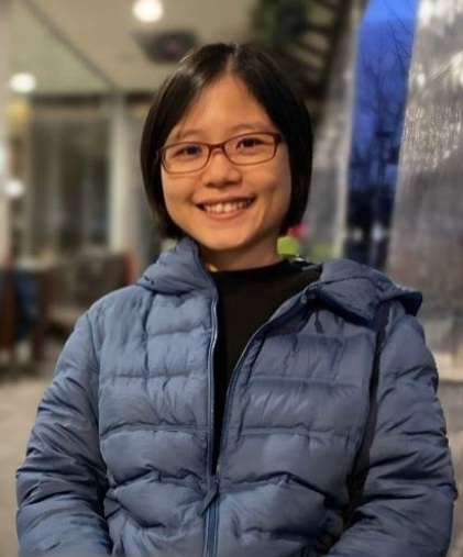
Assoc. Prof. Wei-Sea Chang
Department of Materials Science and Engineering
National Yang Ming Chiao Tung University, Hsinchu, Taiwan
Title of Invited Speech
To be announced
Abstract of Invited Speech
To be announced

Assoc. Prof. Jyoti Jaiswal
Department of Physics, Rajiv Gandhi University
Rono-Hills, Doimukh, Arunachal Pradesh, India
Title of Invited Speech
To be announced
Abstract of Invited Speech
To be announced
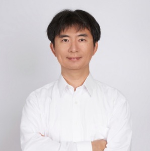
Prof. Chao-Cheng Kaun
Research Center for Applied Sciences, Academia Sinica, Taiwan
Title of Invited Speech
To be announced
Abstract of Invited Speech
To be announced
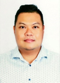
Prof. Ngoc Dang Khoa Tran
Faculty of Mechanical Engineering
Industrial University of Ho Chi Minh City, Vietnam
Title of Invited Speech
To be announced
Abstract of Invited Speech
To be announced
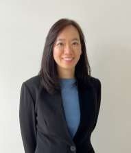
Assoc. Prof. Dr. Teeranoot Chanthasopeephan
Mechanical Engineering Department
King Mongkut's University of Technology Thonburi, Bangkok, Thailand
Title of Invited Speech
From Flexibility to Intelligence: Advancements in Soft Robotics
Abstract of Invited Speech
Recent advancements in robotics and artificial intelligence have brought about a new innovation, driven by the emergence of soft robotics and embedded intelligence. This talk will explore the exciting convergence of these two cutting-edge fields, showcasing how soft robots—known for their flexible, adaptable structures—are redefining applications across industries such as healthcare, agriculture, and beyond.
We will uncover the fundamental principles that make soft robotics unique, including the novel materials and sensors that enable these robots to interact safely and effectively with complex environments. In parallel, we will examine the crucial role of embedded intelligence: the integration of advanced AI algorithms directly into robotic systems, empowering them with real-time perception, autonomous decision-making, and enhanced versatility.
The talk will highlight the latest research trends, and the key challenges that researchers and engineers face when deploying soft robots endowed with intelligent capabilities. By gaining insight into these breakthroughs, we can better imagine a future in which soft, intelligent robots augment human abilities, enhance safety, and deliver smarter, more adaptive automated solutions.
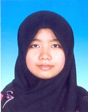
Dr. Nabila A. Karim
Institut Sel Fuel,
University Kebangsaan Malaysia,Malaysia
Title of Invited Speech
To be announced
Abstract of Invited Speech
To be announced

Assoc. Prof. Ratchatin Chancharoen
Mechanical Engineering Department,
Robotics and AI Program Chulalongkorn University, Thailand
Title of Invited Speech
To be announced
Abstract of Invited Speech
To be announced
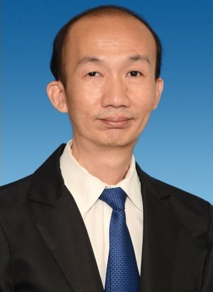
Prof. Dr. Hieng-Kiat Jun
Department of Mechanical and Material Engineering
University Tunku Abdul Rahman, Malaysia
Title of Invited Speech
To be announced
Abstract of Invited Speech
To be announced
 Tel:+886-4-2284-0461 Ext.618